
Tailoring the Optical, Electrical, and Photo-sensing Properties of Chemically Deposited CdS Thin Films through Copper Doping
DOI:
https://doi.org/10.33003/Keywords:
Cadmium sulphide thin films, Copper doping, Chemical bath deposition, Hall-effect measurement, PhotosensorsAbstract
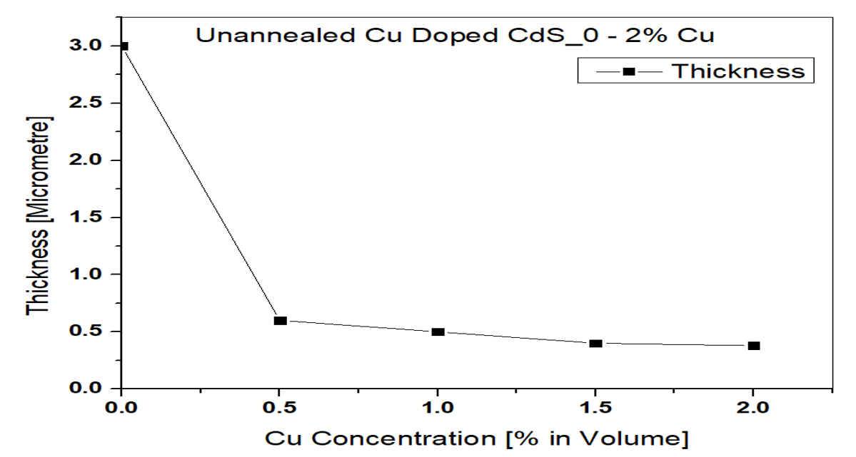
Copper (Cu) doping is an effective approach for tailoring the optoelectronic properties of cadmium sulphide (CdS) thin films for photosensor applications. This study systematically investigates the influence of Cu concentration on the thickness, surface morphology, optical, electrical, and photosensing properties of CdS thin films synthesized by chemical bath deposition. Cu-doped CdS thin films containing 0, 0.5, 1.0, 1.5, and 2.0% (v/v) Cu were deposited under identical conditions to isolate the effect of dopant concentration. Increasing Cu concentration reduced the film thickness from 3.00 to 0.42 μm and the surface roughness from 3029.20 to 67.17 Å, indicating improved film compactness. Optical characterization showed enhanced absorption, extinction coefficient, dielectric response, and optical conductivity, while the optical bandgap increased from 2.07 eV to 2.31 eV at 1.5% Cu. Hall-effect measurements confirmed n-type conductivity for all films, with the highest Hall mobility (1.81 × 10³ cm² V⁻¹ s⁻¹) and the lowest resistivity (1.49 × 10⁴ Ω cm) obtained at 1.5% Cu. The undoped CdS film exhibited the highest photosensitivity (3110.08%) owing to its low dark current, whereas the 0.5% Cu-doped film achieved the highest responsivity (0.0283 mA W⁻¹), indicating the most efficient photodetection performance. Overall, moderate Cu incorporation optimizes the balance between optical absorption, charge transport, and carrier recombination, with 0.5% Cu identified as the optimum concentration for high-performance CdS photosensors. These findings provide valuable insights for the development of low-cost, high-performance CdS-based optoelectronic devices.
References
Abdul-Manaf, N. A., Weerasinghe, A. R., Echendu, O. K., & Dharmadasa, I. M. (2015). Electro-plating and characterisation of cadmium sulphide thin films using ammonium thiosulphate as the sulphur source. Journal of Materials Science: Materials in Electronics, 26, 2418–2429.
Abdullah, M. T., Raoof, L. M., Hasan, M. H., Abd, A. N., & Mohammed, I. M. (2021). The effect of different thickness on the optical and electrical properties of TiO₂ thin films. Journal of Physics: Conference Series, 1999(1), 012128. https://doi.org/10.1088/1742-6596/1999/1/012128
Ali, H. (2022). Advances in chemical bath deposition for metal chalcogenide thin films: A review. Solar Energy Materials and Solar Cells, 246, 111904.
Cai, S., Xu, X., Yang, W., Chen, J., & Fang, X. (2019). Materials and designs for wearable photodetectors. Advanced Materials, 31(18), 1808138.
Corral, R., Ochoa, R., Apolinar, A., & Castillo, S. (2018). Optical and structural properties of ammonia-free CdS:Cu thin film grown on a flexible substrate by the chemical bath method. Chalcogenide Letters, 15, 429–434.
Di Mari, G. M., La Matta, V., Strano, V., Reitano, R., Cerruti, P., Filippone, G., ... & Bruno, E. (2024). Optimized chemical bath deposition for low cost, scalable, and environmentally sustainable synthesis of star-Like ZnO nanostructures. ACS Omega, 9(37), 38591–38598.
Dutta, R., Tian, S. I. P., Liu, Z., Lakshminarayanan, M., Venkataraj, S., Cheng, Y., Bash, D., Chellappan, V., Buonassisi, T., & Jayavelu, S. (2022). Extracting film thickness and optical constants from spectrophotometric data by evolutionary optimization. PLoS ONE, 17(11), e0276555. https://doi.org/10.1371/journal.pone.0276555
Gadallah, A. S., & El-Nahass, M. M. (2013). Structural, optical constants and photoluminescence of ZnO thin films
grown by sol-gel spin coating. Advances in Condensed Matter Physics, 2013, 234546.
Ghediya, P. R., Chaudhuri, T. K., Ray, J., Panjwani, H. L., Hemani, P. J., Paneri, P. P., & Joshi, R. R. (2020). Synthesis and characterizations of copper cadmium sulphide (CuCdS₂) as a potential absorber for thin film photovoltaics. Materials Chemistry and Physics, 252, 123382.
Göde, F. (2019). Effect of Cu doping on CdS as a multifunctional nanomaterial: Structural, morphological, optical and electrical properties. Optik, 197, 163217.
Hakami, J. (2022). Highly induced photosensing behavior of Erbium (Er), Yttrium (Y), and Terbium (Tb) doped nanostructured cadmium sulphide (CdS) thin films prepared by the nebulizer spray pyrolysis method. Journal of Alloys and Compounds, 924, 166577.
Halge, D. I., Narwade, V. N., Khanzode, P. M., Dadge, J. W., Banerjee, I., & Bogle, K. A. (2020). Enhancement in visible light photoresponse of CdS thin films by nitrocellulose surface passivation. ACS Applied Electronic Materials, 2(7), 2151–2154.
Hemathangam, S., Thanapathy, G., & Muthukumaran, S. (2016). Optical, structural, FTIR, and photoluminescence characterization of Cu and Al doped CdS thin films by chemical bath deposition method. Journal of Materials Science: Materials in Electronics, 27, 6800–6808.
Hirpara, J., Malik, G., & Chandra, R. (2022). Optical properties investigation of reactively sputtered tantalum oxynitride films. Materials Today: Proceedings, 57, 202–210.
Inthong, S., Intawin, P., Kraipok, A., Kanthachan, J., Eitssayeam, S., Inthata, U., Denis, S., & Tunkasiri, T. (2019). Investigation of Cu-doped cadmium sulphide photoconductive cells. Engineering Journal Chiang Mai Journal of Science, 46(5), 1009–1014.
Ja’afaru, S., Daniel, I. H., Tanko, Y. A., Kure, N., & Babalola, O. A. (2026). Effect of Deposition Time on the Optoelectronic Properties of CdS Thin Films Synthesized via Chemical Bath Deposition Technique. Physics Access Journal, 6(1), 80–90.
Khimani, A. J., Chaki, S. H., Malek, T. J., Tailor, J. P., Chauhan, S. M., & Deshpande, M. P. (2018). Cadmium sulphide (CdS) thin films deposited by chemical bath deposition (CBD) and dip coating techniques a comparative study. Materials Research Express, 5(3), 036406.
Kukk, P. L., & Altosaar, M. E. (1983). Defect structure of Cl and Cu doped CdS heat treated in Cd and S2 vapor. Journal of Solid State Chemistry, 48(1), 1–10.
Liu, Y., Lian, J., Zhao, M., Wang, Y., Li, M., & Song, H. (2017). The effect of defects on Cu-doped CdS: A first-principles study. Europhysics Letters, 117(5), 57007.
Liu, X., Xu, J., Chen, D., & Shen, G. (2016). Photocatalytic activities of copper-doped cadmium sulfide microspheres prepared by a facile ultrasonic spray-pyrolysis method. Molecules, 21(6), 735.
Liu, X., Wu, M., Li, C., Yu, P., Feng, S., Li, Y., & Zhang, Q. (2022). Interaction structure and affinity of zwitterionic amino acids with important metal cations (Cd²⁺, Cu²⁺, Fe³⁺, Hg²⁺, Mn²⁺, Ni²⁺ and Zn²⁺) in aqueous solution: A theoretical study. Molecules, 27(8), 2407.
Ma, T., Xue, N., Muhammad, A., Fang, G., Yan, J., Chen, R., ... & Sun, X. (2024). Recent progress in photodetectors: From materials to structures and applications. Micromachines, 15(10), 1249.
Mahrov, B., Boschloo, G., Hgfeldi, A., Dloczuk, L., & Diffrich, T. (2004). Photovoltaic study of charge injection from dye molecules into transparent hole and electron conductors. Applied Physics Letters, 84(26), 5455–5457.
Ottih, E., Ekpunobi, A. J., & Ekwo, P. I. (2011). Solid state and optical properties of chemical bath deposited copper nickel sulphide (CuNiS) thin films. The Pacific Journal of Science and Technology, 12(2), 342–347.
Patterson, A. L. (1939). The Scherrer formula for X-ray particle size determination. Physical Review, 56(10), 978–982.
Peng, L., Hu, L., & Fang, X. (2013). Low-dimensional nanostructure ultraviolet photodetectors. Advanced Materials, 25(37), 5321–5328.
Priyadarshini, P., Das, S., & Naik, R. (2022). A review on metal-doped chalcogenide films and their effect on various optoelectronic properties for different applications. RSC Advances, 12(16), 9599–9620.
Rawat, D. K., & Shishodia, P. K. (2016). Growth of ZnO thin films doped with (Mn & Co) by spin coating technique. In AIP Conference Proceedings (Vol. 1728, No. 1, Article 020256).
Shannon, R. D. (1976). Revised effective ionic radii and systematic studies of interatomic distances in halides and chalcogenides. Acta Crystallographica Section A, 32(5), 751–767.
Sharma, J., Mishra, M., Jain, S., & Tripathi, B. (2022). Tuning of structural, optical and electrical characteristics of Cu/CdS composite thin films for energy applications. International Journal of Advances in Engineering and Management, 4, 507–517.
Shkir, M., Khan, Z. R., Anis, M., Shaikh, S. S., & AlFaify, S. (2020). A comprehensive study of opto-electrical and nonlinear properties of Cu@CdS thin films for optoelectronics. Chinese Journal of Physics, 63, 51–62.
Toma, F. T. Z., Rahman, S., Hussain, K. M. A., & Ahmed, S. (2024). Thin film deposition techniques: A comprehensive review. J Mod Nanotechnol, 4(6).
Zaker, T., Aziz, N., Mohammed, A., Haneen, K., Fadhil, N., & Salman, S. (2021). Synthesis of nanocrystalline cadmium sulphide film and the influence of Cu doping on the physical characterization. Journal of Nanostructures, 11, 269–275.
Zhou, J., Yang, Y., & Zhang, C. Y. (2015). Toward biocompatible semiconductor quantum dots: From biosynthesis and bioconjugation to biomedical application. Chemical Reviews, 115(21), 11669–11717.
Downloads
Published
Issue
Section
Categories
License
Copyright (c) 2026 Simon Ja'afaru, Hyuk Daniel Isaac, Yakubu Aliyu Tanko, Nicodemus Kure, Thomas Ivie Imalerio, Yusuf Alhassan

This work is licensed under a Creative Commons Attribution 4.0 International License.