
GROWTH AND CHARACTERIZATION OF INDIUM OXIDE MICROSTRUCTURES USING CHEMICAL VAPOUR DEPOSITION METHOD
DOI:
https://doi.org/10.33003/fjs-2026-1006-5172Keywords:
Indium Oxide, Thin film, Microstructures, Nanostructures, Bandgap energyAbstract
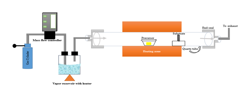
Indium oxide (In₂O₃) thin films are typically deposited on quartz, sapphire, and silicon substrates by chemical vapour deposition (CVD) because of the high temperatures required during film growth. In this study, however, high-quality In₂O₃ thin films were successfully deposited on glass substrates using the CVD technique. The source temperature was varied from 850 °C to 1000 °C, while the substrates were positioned downstream in a lower-temperature region maintained between 400 °C and 500 °C. The morphological, structural, and optical properties of the deposited films were characterized using field-emission scanning electron microscopy (FESEM), X-ray diffraction (XRD), and UV–Visible spectrometry, respectively. The results revealed significant temperature-dependent changes in the film morphology, accompanied by improved crystallinity at higher deposition temperatures. Optical studies further showed a reduction in the optical bandgap from 3.470 eV to 3.021 eV with increasing growth temperature. These findings demonstrate that controlled downstream CVD growth provides an effective route for synthesizing crystalline In₂O₃ thin films on low-cost glass substrates with tunable optical properties.
References
Ahmed, N. M., Sabah, F. A., Abdulgafour, H. I., Alsadig, A., Sulieman, A., & Alkhoaryef, M. (2019). The effect of post annealing temperature on grain size of indium-tin-oxide for optical and electrical properties improvement. Results in Physics, 13(February), 102159. https://doi.org/10.1016/j.rinp.2019.102159
Aper, T M, Yam, F. K., Saw, K. G., Poay, K., & Chahrour, K. M. (2021). Results in Physics Atmospheric pressure chemical vapor deposition of indium oxide nanostructured films for photoelectrochemical application. Results in Physics, 24(April), 104187. https://doi.org/10.1016/j.rinp.2021.104187
Aper, T Moses, Tyona, M. D., Yam, F. K., & Beh, K. P. (2023). Structural and Optical Characterization of Electrochemically Deposited Indium Oxide Nanostructures for Photoelectrochemical Investigation. https://doi.org/10.1021/acs.cgd.2c01185
Domènech-Gil, G., Barth, S., Samà, J., Pellegrino, P., Gràcia, I., Cané, C., & Romano-Rodriguez, A. (2017). Gas sensors based on individual indium oxide nanowire. Sensors and Actuators, B: Chemical, 238, 447–454. https://doi.org/10.1016/j.snb.2016.07.084
Džimbeg-Malčić, V., Barbarić-Mikočević, Ž., & Itrić, K. (2011). Kubelka-Munk theory in describing optical properties of paper (I). Tehnički Vjesnik : Znanstveno-Stručni Časopis Tehničkih Fakulteta Sveučilišta u Osijeku, 18(1), 117–124.
Elam, J. W., Martinson, A. B. F., Pellin, M. J., & Hupp, J. T. (2006). Atomic layer deposition of in 2O 3 using cyclopentadienyl indium: A new synthetic route to transparent conducting oxide films. Chemistry of Materials, 18(15), 3571–3578. https://doi.org/10.1021/cm060754y
Gan, J., Lu, X., Wu, J., Xie, S., Zhai, T., Yu, M., Zhang, Z., Mao, Y., Wang, S. C. I., Shen, Y., & Tong, Y. (2013). Oxygen vacancies promoting photoelectrochemical performance of in 2 O 3 nanocubes. Scientific Reports, 3, 1–7. https://doi.org/10.1038/srep01021
Her, S.-C., & Chang, C.-F. (2017). Fabrication and characterization of indium tin oxide films. Journal of Applied Biomaterials & Functional Materials, 15(2), 0–0. https://doi.org/10.5301/jabfm.5000345
Hosseini, a, Icli, K. C., & Güllü, H. H. (2013). Preparation and characterization of porous TiO 2 thin films by sol-gel method for Extremely Thin Absorber-ETA solar cell applications Çok ince Soğurucu – ETA g üneş gö zeler e uygulamaları için gö zenekli TiO 2 ince filmlerin sol-jel metodu ile ü retilmes. Turkish Journal of Science & Technology, 8(2), 69–79.
Jubu, P. R., Aper, T. M., & Igba, V. M. (n.d.). Growth Mechanism and Structural Elucidation of Indium Oxide Microstructures Prepared by Carbothermal and Hydrogen Reduction Processes.
Jubu, P. R., Yam, F. K., & Moses, A. T. (2020). Deposition of Gallium Oxide Nanostructures at Low Substrate Temperature by Chemical Vapor Deposition. ECS Journal of Solid State Science and Technology, 9(3), 035006. https://doi.org/10.1149/2162-8777/ab7b47
Karazhanov, S. Z., Ravindran, P., Vajeeston, P., Ulyashin, A., Finstad, T. G., & Fjellvåg, H. (2007). Phase stability, electronic structure, and optical properties of indium oxide polytypes. Physical Review B - Condensed Matter and Materials Physics, 76(7), 1–13. https://doi.org/10.1103/PhysRevB.76.075129
Karn, A., Kumar, N., & Aravindan, S. (2017). Chemical vapor deposition synthesis of novel indium oxide nanostructures in strongly reducing growth ambient. Journal of Nanostructures, 7(1), 64–76. https://doi.org/10.22052/jns.2017.01.008
King, P. D. C., Veal, T. D., Fuchs, F., Wang, C. Y., Payne, D. J., Bourlange, A., Zhang, H., Bell, G. R., Cimalla, V., Ambacher, O., Egdell, R. G., Bechstedt, F., & McConville, C. F. (2009). Band gap, electronic structure, and surface electron accumulation of cubic and rhombohedral In2 O3. Physical Review B - Condensed Matter and Materials Physics, 79(20), 1–10. https://doi.org/10.1103/PhysRevB.79.205211
Lei, F., Sun, Y., Liu, K., Gao, S., Liang, L., Pan, B., & Xie, Y. (2014a). Oxygen vacancies confined in ultrathin indium oxide porous sheets for promoted visible-light water splitting. Journal of the American Chemical Society, 136(19), 6826–6829. https://doi.org/10.1021/ja501866r
Lei, F., Sun, Y., Liu, K., Gao, S., Liang, L., Pan, B., & Xie, Y. (2014b). Oxygen vacancies confined in ultrathin indium oxide porous sheets for promoted visible-light water splitting. Journal of the American Chemical Society, 136(19), 6826–6829. https://doi.org/10.1021/ja501866r
Li, C., Zhang, D., Han, S., Liu, X., Tang, T., Lei, B., Liu, Z., & Zhou, C. (2003). Synthesis, Electronic Properties, and Applications of Indium Oxide Nanowires. Annals of the New York Academy of Sciences, 1006(2), 104–121. https://doi.org/10.1196/annals.1292.007
Li, Chao, Zhang, D., Liu, X., Han, S., Tang, T., Han, J., & Zhou, C. (2003). In2O3 nanowires as chemical sensors. Applied Physics Letters, 82(10), 1613–1615. https://doi.org/10.1063/1.1559438
Li, Conan, & Han, S. (2003). Ultraviolet photodetection properties of indium oxide nanowires. January 2016. https://doi.org/10.1007/s00339-003-2099-3
Liang, C. H., Meng, G. W., Lei, Y., Phillipp, F., & Zhang, L. D. (2001). Catalytic growth of semiconducting In2O3 nanofibers. Advanced Materials, 13(17), 1330–1333. https://doi.org/10.1002/1521-4095(200109)13:17<1330::AID-ADMA1330>3.0.CO;2-6
Ma, Q., Zheng, H. M., Shao, Y., Zhu, B., Liu, W. J., Ding, S. J., & Zhang, D. W. (2018). Atomic-Layer-Deposition of Indium Oxide Nano-films for Thin-Film Transistors. Nanoscale Research Letters, 13(1). https://doi.org/10.1186/s11671-017-2414-0
Mahalingam, S., & Abdullah, H. (2016). Electron transport study of indium oxide as photoanode in DSSCs: A review. Renewable and Sustainable Energy Reviews, 63, 245–255. https://doi.org/10.1016/j.rser.2016.05.067
Piper, L. F. J., Demasi, A., Cho, S. W., Smith, K. E., Fuchs, F., Bechstedt, F., Körber, C., Klein, A., Payne, D. J., & Egdell, R. G. (2009). Electronic structure of In2 O3 from resonant x-ray emission spectroscopy. Applied Physics Letters, 94(2), 1–4. https://doi.org/10.1063/1.3070524
Qurashi, A., Irfan, M. F., & Alam, M. W. (2010). In2O3 nanostructures and their chemical and biosensor applications. Arabian Journal for Science and Engineering, 35(1 C), 125–145.
Ray, S., Banerjee, R., Basu, N., Batabyal, A. K., & Barua, A. K. (1983). Properties of tin doped indium oxide thin films prepared by magnetron sputtering. Journal of Applied Physics, 54(6), 3497–3501. https://doi.org/10.1063/1.332415
Sakaliuniene, J., Čyviene, J., Abakevičiene, B., & Dudonis, J. (2011). Investigation of structural and optical properties of GDC thin films deposited by reactive magnetron sputtering. Acta Physica Polonica A, 120(1), 63–65. https://doi.org/10.12693/APhysPolA.120.63
Stroescu, H., Anastasescu, M., Preda, S., Nicolescu, M., Stoica, M., Stefan, N., Kampylafka, V., Aperathitis, E., Modreanu, M., Zaharescu, M., & Gartner, M. (2013). Influence of thermal treatment in N2 atmosphere on chemical, microstructural and optical properties of indium tin oxide and nitrogen doped indium tin oxide rf-sputtered thin films. Thin Solid Films, 541(February), 121–126. https://doi.org/10.1016/j.tsf.2012.11.135
Yahia, A., Attaf, A., Saidi, H., Dahnoun, M., Khelifi, C., Bouhdjer, A., Saadi, A., & Ezzaouia, H. (2019). Structural, optical, morphological and electrical properties of indium oxide thin films prepared by sol gel spin coating process. Surfaces and Interfaces, 14(October 2018), 158–165. https://doi.org/10.1016/j.surfin.2018.12.012
Zhang, Q., Wang, S., Fu, H., Wang, Y., Yu, K., & Wang, L. (2020). Facile Design and Hydrothermal Synthesis of In 2 O 3 Nanocube Polycrystals with Superior Triethylamine Sensing Properties. https://doi.org/10.1021/acsomega.0c00497
Downloads
Published
Issue
Section
Categories
License
Copyright (c) 2026 Tewrase M. Aper, Jonathan T. Ikyumbur, Augustine A. McAsule, Paul S. Amon, Oluwatosin S Obaseki

This work is licensed under a Creative Commons Attribution 4.0 International License.

