FIRST-PRINCIPLES INVESTIGATION OF THE ELECTRONIC STRUCTURE AND OPTICAL RESPONSE OF Ga2S3 AND Ga2Se3 CHALCOGENIDES
DOI:
https://doi.org/10.33003/fjs-2025-0911-4018Keywords:
Pseudopotential, Dielectric Function, LDA+U, Density of States, Binary MaterialsAbstract
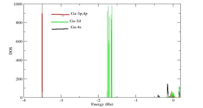
Gallium sulfide (Ga₂S₃) and gallium selenide (Ga₂Se₃) vacancy defect binary materials in the monoclinic Cc phase with a four formula units in a unit cell have been investigated within the density functional theory (DFT) framework. DFT (LDA +U), with PAW pseudopotentials in the Abinit (v7.10); plane-wave cut-off of 15 Ha, k-point grid of 4x4x4 were used in the calculations. Both Ga₂S₃ and Ga₂Se₃ were identified as semiconductors, exhibiting direct band gaps at the Γ- point, with values of 2.86 eV ( and 1.47 eV , respectively. These results are in agreement with the experimental values of Ga₂S₃ 2.48 eV (Işık et al, 2018) and Ga₂Se₃ 1.99 eV (Huang, 2013). Orbital contributions to the DOS reveal that, in Ga₂S₃, the VBM is dominated by S-3s states, whereas the CBM is mainly derived from Ga-4s and S-3p states. In Ga₂Se₃, the VBM arises chiefly from Se-4s states, while the CBM is primarily composed of Ga-3d and Se-4p states. Dielectric response function calculations yielded (0) of 4.9 and 6.0 for Ga₂S₃ and Ga₂Se₃ respectively. These narrow bandgaps enable efficient absorption in the visible range for solar energy conversion and light-emitting applications. The results offer a theoretical foundation for additional experimental research on these materials. It is recommended that temperature-dependence and optical absorption spectra be investigated using other computational methods to assess optoelectronic applications.
References
Gonze X., Beuken J.-M., Caracas R., Detraux F., Fuchs M., Rignanese G.-M., Sindic L., Verstraete M., Zerah G., Jollet F., Torrent M., Roy A., Mikami M., Ghosez Ph., Raty J.-Y., and Allan D.C., (2002) First-principles computation of material properties: the Abinit software project. Computational Materials Science. 25, 478-492.
Gonze X., Rignanese G.-M., Verstraete M., Beuken J.-M., Pouillon Y., Caracas R., Jollet F., Torrent M., Zerah G., Mikami M., Ghosez Ph., Veithen M., Raty J.-Y., Olevano V., Bruneval F., Reining L., Godby R., Onida G., Hamann D. R., and Allan D. C., (2005) A brief Introduction to the Abinit software package. Z. Kristallogr. 220, 558-562.
Güler, I., Işıkhan, M., Hasanlı, N., Gasanova, L. & Babayeva, R. (2019). Structural and optical properties of Ga₂Se₃ crystals by spectroscopic ellipsometry. Journal of Electronic Materials. 48(4), 2418 – 2422.
He, J., Tian, Z., Wang, Y., & Guo, S. (2017). First-principles study of structural and electronic properties of Ga₂S₃ polymorphs. Journal of Alloys and Compounds, 705, 452–459.
Ho, C. H. (2020). Ga₂Se₃ Defect Semiconductors: The Study of Direct Band Edge and Optical Properties. ACS Omega, 5 18527 – 18534.
Ho, C. H., & Chen, H. H. (1999). Optically decomposed near-band-edge structure and excitonic transitions in Ga₂S₃. Journal of Crystal Growth, 207(1-2), 69–76.
Huang, G.-Y., Abdul Jabbar, N. M., & Wirth, B. D. (2013). First Principles Study of the Structure and Band Structure of Ga₂Se₃. Journal of Physics. Condensed Matter, 25(22), 225503.
Huang, G.-Y., Abdul Jabbar, N. M., & Wirth, B. D. (2014). Theoretical study of Ga₂Se₃, Ga₂Te₃ and Ga₂(Se₁ ₓTeₓ)₃: Band gap engineering. Acta Materialia, 71, 349–369.
Işık, M., Hasanli, N., & Gasanova, L. (2018). Spectroscopic ellipsometry investigation of optical properties of beta Ga₂S₃ single crystals. Optical Materials. 86, 95 – 99.
Işık, M., Hasanli, N., & Gasanova, L. (2019). Optical Properties of (Ga₂Se₃) (0.75) – (Ga₂S₃)(0.25) Single Crystals by Spectroscopic Ellipsometry. Physica B. Condensed Matter, 560: 6-10.
Madelung, O. (2004). Semiconductors: Data Handbook, Springer, 3rd Edition. 275.
Mathew, F., Poonkottil, N., Solano, E., Poelman, D., & Dendooven, J. (2023). Plasma enhanced atomic layer deposition of crystalline Ga₂S₃ thin films. J. Vac. Sci. & Technol. A41. 060401, 1 – 7.
Meng, X., Libera, J. A., Fister, T. T., Zhou, H., Hedlund, J. K., Fenter, P. & Elam, J. W.(2014). Atomic Layer Deposition of Gallium Sulfide Films using Hexakis (dimethyiamido) digallium and Hydrogen Sulfide. Chemistry of Materials. 26(2): 1029 – 1039.
Omehe, N. N., &Nwachuku, D. N. (2021). Electronic Properties of the Chalcopyrites AgFeS2, AgFeSe2 and AgFeTe2 Compounds. Advanced Material Letters, 12(1), 21011597.
Park, J., Lee, H., & Kim, D. (2020). Gallium vacancy engineering in Ga₂S₃ for enhanced optoelectronic properties. Journal of Materials Chemistry C, 8, 12315–12322.
Park, K., Kim, D. T., Debela, T. T., Boujnah, M., Zewdie, G. M., Seo, J., Kwom, I. S., Kwak, I. H., Jung, M., Park, J. & Kang, H. S. (2022). Polymorphic Ga₂S₃ nanowires: Phase controlled growth and crystal structure calculations. Nanoscale Advances, 4(15), 3218–3225.
Perdew, J. P. & Zunger, A. (1981). Self-Interaction Correction to Density-Functional Approximations for Many-Electron Systems. Physical Review B, 23(10), 5048 – 5079.
Ueno, K., Kawayama, M., Dai, Z. R., Koma, A., & Ohuchi, F. S. (1999).Growth and Characterization of Ga₂Se₃/GaAs (100) Epitaxial Thin Films. Journal of Crystal Growth, 207, 69–76.
Wang, K., Ye, W., Yin, W., Chai, W., Rui, Y. & Tang, B. (2019). A Novel Carbon-Coated Ga₂S₃ Anode Material derived from Post-Synthesis Modified MOF for High-Performance Lithium Ion and Sodium Ion Batteries. Electrochim Acta. 322: 134790
Zheng, Y., Tang, X., Wang, W., Jin, L. & LI. G. (2021). Large-Sized Ultrathin a- Ga₂S₃ Nanosheets toward High-Performance Photodetection. Advanced Functional Materials, 31(6): 2008307
Zhou, Y., Liu, Q., Yan, Y. (2019). Band structure engineering of Ga₂Se₃ for high-performance photovoltaics. Advanced Materials, 31(2), 1805522.
Downloads
Published
Issue
Section
Categories
License
Copyright (c) 2025 Doris Ngozi Nwachuku

This work is licensed under a Creative Commons Attribution 4.0 International License.

